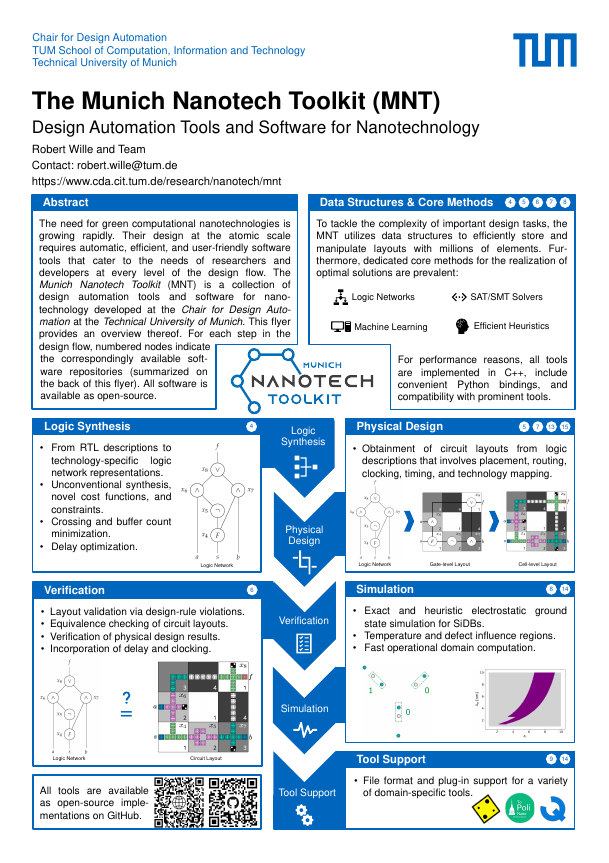
The Munich Nanotech Toolkit (MNT) is a collection of design automation tools and software for various nanotechnologies developed at the Chair for Design Automation at the Technical University of Munich. The tools encompass state-of-the-art methods for design tasks including but not limited to logic synthesis, physical design, verification, and physical simulation. These are additionally integrated into design flows covering the entire nanotechnology design stack.
All the software is available as open-source implementations and is hosted on GitHub (see the following links). This page first provides a brief introduction to the core MNT framework fiction , which can be used to execute the different flows (i.e., realizes a flow for logic synthesis, one for physical design, and one for simulation). Afterward, we provide overviews of the physical design tool MNT NanoPlaceR , the co-design tool MNT Designer , and the benchmark suite MNT Bench .
A Framework for Nanotechnology
Lying at the heart of the MNT, the fiction framework serves as the foundation for Nanotech Design Automation. Providing powerful and versatile C++ API and Python bindings , fiction serves as a base for our research as well as first- and third-party tools. Additionally, fiction can be used as a Command-line Interface (CLI) that enables the swift access to any part of the nanotechnology design stack for researchers and developers alike. Furthermore, its setup for experimental evaluations makes sharing evaluation scripts for reproducible research findings a breeze. With these features, you can easily explore the world of Nanotech Design Automation.
The following goes into further details of each design flow that can be realized/executed on top of fiction and explains corresponding supplementary MNT tools. For more information on installation and usage, we refer to the online documentation .
The Logic Synthesis Flow
Conventional logic synthesis aims at CMOS technologies where wire costs can be almost neglected. In nanotechnology, however, wire segments are fabricated from the same building blocks as gates and share both their area requirements and delay properties. Our logic synthesis approaches, thus, consider wire costs to obtain area and delay efficient circuit layouts.
Key Features
-
Specialized Synthesis: Within the nanotechnology landscape, we offer specialized synthesis techniques, that also support Majority (MAJ) synthesis. These techniques are fine-tuned to address the unique requirements and challenges presented by nanoscale logic circuits.
-
Delay Optimization: Recognizing the significance of precise timing in nanotech circuits, our logic synthesis flow includes delay optimization strategies. These optimizations ensure that your designs not only meet logical requirements but also exhibit the desired timing characteristics.
Tool Compatibility
-
File Compatibility: fiction boasts excellent flexibility in input formats for your design specifications. It is capable of parsing Verilog, AIGER, and BLIF files, allowing you to work with your preferred format, ensuring a seamless transition into the nanotechnology design process.
-
Integration with mockturtle : The provided logic synthesis flow seamlessly integrates with mockturtle, enhancing the range of available synthesis options. This collaboration provides access to a comprehensive set of synthesis tools, further enriching your nanotechnology design capabilities.
-
Optimization via ABC : Prior to the logic synthesis flow, you have the option to leverage the powerful ABC tool to synthesize and optimize netlists. This additional layer of optimization can significantly streamline the design process and enhance the quality of the circuits synthesized for nanotechnology applications.
Utilizing the flow
- Simply pass the CMake flag
-DFICTION_LOGIC_SYNTHESIS_FLOW=ONto configure fiction for logic synthesis.
The Physical Design Flow
Physical Design involves mapping an input netlist onto a layout while respecting all constraints imposed by the target technology. In the domain of nanotechnology, these constraints frequently involve clocking and data synchronization problems that pose unique challenges that require specialized solutions. Conventional physical design methodologies often fall short in accommodating its intricacies. Our physical design approaches are specifically developed with these particular constraints in mind.
Key Features
-
Technology-independent Algorithms: All physical design algorithms abstract from physical implementations while preserving common traits of underlying technologies. Thereby, they deliver versatility for various scenarios. Resulting gate-level layouts can be mapped to technology-specific implementations in a straight-forward post-processing step via the application of a gate library. Currently supported technologies include Quantum-dot Cellular Automata (QCA), Nanomagnet Logic (NML), and Silicon Dangling Bonds (SiDBs).


-
Customized Placement & Routing: The provided physical design flow offers tailored placement and routing algorithms, designed to address the specific constraints and characteristics of nanotech circuit layouts.
-
Exact and Heuristic Design Options: We understand that not all design scenarios require the same level of precision. The physical design flow provides options for both exact and heuristic design solutions. Whether you need optimal layouts at the cost of runtime or rapid, yet effective designs, want to unleash the power of deep reinforcement learning (see also the section about NanoPlaceR ), or even require layouts based on different cost objectives , this flow has you covered.
-
Specialized Routing: Routing in nanotech circuit layouts is complex due to their unique planar nature. Our research has led to the development of specialized routing techniques, ensuring efficient signal connection even in convoluted cases.
-
Post-Layout Optimization: Manually or automatically designed nanotech circuit layouts might be non-optimal with hidden potential for optimization. A post-layout optimization algorithms can unearth overlooked capacity for gaining both area and delay efficiency.
-
Layout Validation: To ensure logical correctness under data synchronization constraints, we offer layout validation methodologies that include design-rule violation and equivalence checking via formal methods. These enable the verification of layouts with hundreds of millions of tiles within seconds.
-
Gate Libraries: After technology-independent physical design, the obtained layouts can be mapped to technology-specific implementations using gate established libraries. We offer support for a variety of libraries including QCA ONE , ToPoliNano , and Bestagon .
Tool Compatibility
-
QCADesigner : CAD, layout visualization, and physical simulation of QCA circuits.
-
ToPoliNano & MagCAD : EDA and hierarchical layout design for iNML circuits. Layout visualization and physical simulation of mQCA, iNML, and pNML circuits.
-
SiQAD : CAD, layout visualization, and physical simulation of SiDB circuits.
-
SCERPA : Physical simulation of mQCA circuits.
-
QCA-STACK : Design and discrete simulation of (stackable) QCA circuits.


CLI Demo

Utilizing the Flow
- Simply pass the CMake flag
-DFICTION_PHYSICAL_DESIGN_FLOW=ONto configure fiction for physical design.
The Simulation Flow
Physical simulation in the nanotechnology domain is a critical step before fabrication takes places. Due to high manufacturing cost that partially involve manual labor, any layout obtained from the previous physical design flow must be carefully simulated under realistic physical assumptions to ensure its operability in real-world conditions. The resulting simulation tasks regularly constitute high-dimensional optimization problems of exponential complexity to capture quantum-physical phenomena. Our simulation engines address this complexity via sophisticated methods such as physically-informed search space pruning, partial solution caching, and effective state enumeration.
Key Features
-
Electrostatic Ground-State Simulation: The provided simulation techniques enable the accurate analysis of electrostatic ground states , providing critical insights into the behavior of SiDB devices at low temperatures. This step is essential for determining logical circuit behavior and revealing design flaws.
-
Temperature Simulation: SiDBs operate in a domain where temperature effects can significantly impact device performance. The simulation flow includes temperature modeling , allowing designers to evaluate the behavior of SiDB circuits under various thermal conditions, potentially revealing kinks undetectable at low temperature.
-
Atomic Defect Simulation: In the SiDB landscape, even atomic-scale material defects can have a profound impact on device functionality and/or manufacturability. The simulation approaches incorporate atomic defect modeling, enabling the assessment of device behavior in the presence of imperfections at the atomic scale.
-
Operational Domain Analysis: Single physical simulation runs only provide a glimpse into an SiDB layout’s behavior under very specific material property values. However, these properties are often sample-specific and thus may vary. An Operational Domain Analysis performs a sweep of physical simulations over a parameter range, providing a more detailed picture of layout correctness. Our Operational Domain algorithms require substantially fewer simulator calls than any state-of-the-art algorithm while maintaining the same resolution.
Tool Compatibility
While all these simulation engines are implemented as part of fiction, the SiQAD GUI can be utilized to invoke them on any SiDB layout. For this use case, we offer our simulators as plugins for SiQAD . Via fiction’s file support for SiQAD layout files, also automatically obtained layouts from the previous physical design flow can be inspected, edited, and simulated in SiQAD with the power of these effective physical simulators.
Utilizing the Flow
- Simply pass the CMake flag
-DFICTION_SIMULATION_FLOW=ONto configure fiction for simulation.
MNT NanoPlaceR
MNT NanoPlaceR is a tool for the physical design of FCN circuitry based on reinforcement learning, which can generate layouts for logic networks up to ~200 gates, while requiring ~50% less area than the state-of-the-art heuristic approach.
Inspired by recent developments in the field of machine learning-aided design automation, this tool combines reinforcement learning with efficient path routing algorithms based on established algorithms such as A* search. Masked Proximal Policy Optimization (PPO) is used to learn the placement of logic elements, which is further accelerated by incorporating an action mask computed based on the netlist structure and the last partial placement, ensuring valid and compact solutions. To minimize the occurrence of unpromising partial placements, several checks constantly ensure the early termination of sub-par solutions. Furthermore, the routing of placed gates is incorporated directly into the placement step using established routing strategies.
MNT Designer
MNT Designer is a comprehensive, fully open-source, GUI-based tool that advances the design of FCN circuits from high-level logic specifications through to fabrication-ready, cell-level layouts. By unifying previously separate stages such as physical design, “on-the-fly” gate design, and verification in a graphical user interface, the tool streamlines an otherwise fragmented workflow. Specifically, it enables researchers and designers to import and edit high-level logic descriptions, generate and refine gate-level layouts, verify design-rule compliance, and export completed designs for simulation and fabrication. The modularity and scalability of the proposed approach accommodate both exact and heuristic algorithms, offering flexibility in tackling the wide range of problems and constraints inherent to FCN technologies. The ability to manually adjust layouts alongside automated post-layout optimization algorithms further empowers experts to explore custom solutions for performance-critical or domain-specific designs. Moreover, the integrated gate-design functionality for SiDBs facilitates rapid prototyping and testing of new concepts. Overall, by integrating these capabilities into a single, user-friendly environment, the presented tool fills a critical gap in existing FCN design tools. It thereby accelerates research and development in nanoscale computing, ultimately paving the way for more efficient, reliable, and scalable FCN circuits.
MNT Bench
Software tools and methods require practical and relevant benchmarks to compare them to the current state of the art. In order to aid researchers and developers in this task, we provide MNT Bench —a benchmark suite that includes layouts for multiple abstraction levels, gate libraries, clocking schemes, physical design algorithms, and optimizations to empirically evaluate and compare software and design automation tools for nanotechnologies.
- Simply pass the CMake flag